The Silent Revolution: TSMC Begins Mass Production of 2nm Chips


As we count down the final hours of 2025, a monumental event just took place in the tech world. It wasn’t marked by fireworks or a flashy keynote presentation. Instead, the world’s semiconductor giant, TSMC, has officially kicked off mass production of its long-awaited 2-nanometer (N2) process.
What strikes me the most isn’t just the technology itself, but how they did it. No press release, no CEO speech, no confetti. They simply updated a status on their website. That is what I call “quiet confidence.”
So, why does this “2nm” milestone matter for the phone in your pocket or the AI models we use daily? Let’s dissect this silent revolution from the heart of Silicon Valley to the fabs in Taiwan.
Why the Silence?

TSMC had previously whispered that mass production would start in the fourth quarter of this year. Usually, when a company hits a milestone this big, they shout it from the rooftops. TSMC’s silence tells me one thing: the machines are humming, and the yields are good.
This lack of fanfare suggests that the initial batches—likely destined for future Apple (iPhone 18 Pro, perhaps?) and Nvidia hardware—are already moving along the assembly line. The countdown to the next generation of computing has technically begun.
The Numbers Game: What Does N2 Give Us?

I dug into the technical specs so you don’t have to. When we compare N2 to the current N3E (3nm) generation, the improvements are significant. For those asking, “Will my phone get faster?”, here is the breakdown:

- More Speed: A 10% to 15% performance boost at the same power consumption.
- Better Efficiency (The Real Winner): A 25% to 30% reduction in power consumption at the same speed.
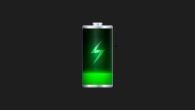
This is the part that excites me. Processors are already fast enough for 99% of us. But battery life? That is where we are all starving. TSMC is essentially saying, “Your device can run just as fast, but it will sip 30% less juice.” That is a game-changer for mobile devices.
The Tech Shift: Goodbye FinFET, Hello GAA!
Here is the “geeky” part, but stay with me because it’s historic. For years, the industry relied on FinFET transistor architecture. But as chips got smaller, FinFET hit a physical wall.
With N2, TSMC is finally switching to Gate-All-Around (GAA) nanosheet technology. Think of it this way: In the old design, the “gate” (the switch that controls electricity) grabbed the channel from three sides. In GAA, the gate surrounds the channel on all four sides.
- The Result: Total control over the current, zero leakage, and higher density.
They also introduced something called SHPMIM (Super High Performance Metal-Insulator-Metal) capacitors. It sounds like a mouthful, but it basically means they doubled the capacity stability within the chip. It’s not just the transistors that evolved; the power veins feeding them did too.
The Roadmap: A16 and N2P are Next
TSMC isn’t stopping here. While the N2 lines are running, the roadmap for 2026 is already set:
- H2 2026: We will see N2P (a polished version of N2) and the highly anticipated A16 node.
- A16 Magic: This will introduce “Super Power Rail” technology, moving power delivery to the back of the chip to save space and reduce interference.
My Final Thoughts
We are living in an era where software (specifically AI) is hungry for power. It pushes hardware to its breaking point. TSMC’s move to 2nm is hardware’s way of saying, “I can handle this.”
This silent launch impresses me more than any loud marketing campaign ever could. It’s pure engineering muscle.
I have to ask: Would you prefer that 15% extra speed, or are you like me—desperate for that 30% extra battery life? Let me know in the comments!