
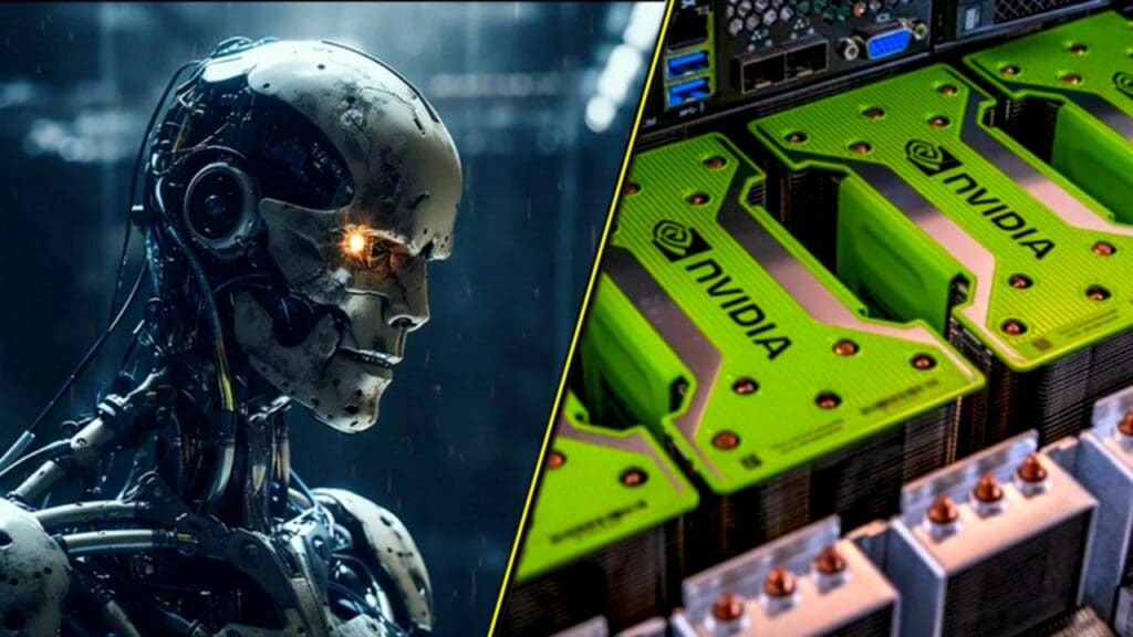
Nvidia is preparing to change the rules of physics in computing. The upcoming “Feynman” GPU architecture isn’t just an upgrade; it’s a structural revolution featuring 3D stacking and Groq’s LPU technology.
The future of artificial intelligence is shifting from “learning” to “doing,” and Nvidia’s hardware roadmap is adapting to this reality. New details have emerged about the company’s post-2028 architecture, codenamed Feynman, which promises to integrate Groq’s Language Processing Unit (LPU) technology directly into the GPU using advanced 3D stacking methods.
The Hybrid Future: GPU Meets LPU
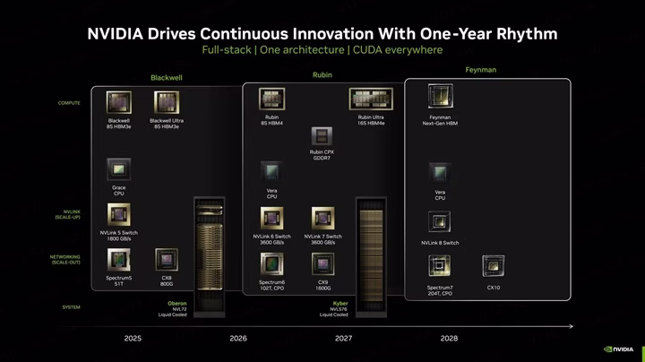
According to recent leaks and insights from GPU expert AGF, Nvidia is exploring a design philosophy similar to AMD’s X3D technology but for AI inference. The plan involves stacking LPU units—dedicated chips for language processing—directly on top of the main GPU die using TSMC’s SoIC hybrid bonding technology.
This move addresses a critical bottleneck in modern chip manufacturing: SRAM scaling.
- The Problem: Integrating massive amounts of SRAM (memory) directly into the main processor die is becoming inefficient and costly at advanced nodes like 1.6nm (A16).
- The Solution: By separating the LPU and its large SRAM cache into a distinct layer and stacking it vertically, Nvidia can maximize performance while keeping energy consumption low. This allows the main “Feynman” compute die to be manufactured on the cutting-edge A16 process, while the memory-heavy LPU layer handles the high-speed data access required for AI agents.
Engineering Challenges: Heat and Software

This ambitious leap is not without its risks. Stacking powerful compute units creates a significant thermal challenge. LPUs operate with a constant, high-throughput workload, generating immense heat that could throttle the entire system if not managed correctly.
Furthermore, there is a software hurdle. Nvidia’s dominance is built on CUDA, a software ecosystem designed for hardware abstraction. LPUs, however, typically require explicit memory management. Merging these two conflicting philosophies will require Nvidia to rewrite the rulebook on how software talks to hardware.

🧠 Metaverse Planet Perspective: Why This Matters?
As we analyze this development, it’s clear that Nvidia is preparing for the “Age of Inference.”
For the past decade, the focus has been on training massive AI models (like GPT-4). But in the future (2028 and beyond), the focus will shift to running billions of AI agents simultaneously in real-time. That is where the Feynman architecture comes in.
- The “Thinking” Chip: By integrating Groq’s LPU technology, Nvidia isn’t just making a faster calculator; they are building a chip designed to “speak” and “understand” natively. This is the hardware required for the true Human 2.0 experience—where your AI assistant responds instantly, with zero latency.
- Beyond Moore’s Law: The shift to 3D stacking proves that we are reaching the physical limits of traditional 2D chips. The future is vertical. Nvidia is literally building skyscrapers on silicon to fit the intelligence of the future into a tiny square.
Bottom Line: The Nvidia Feynman is not just a graphics card; it is the potential engine of the Metaverse, designed to power a world where every object and digital entity has its own intelligence.